

ADC Add-on Board
Table of Contents
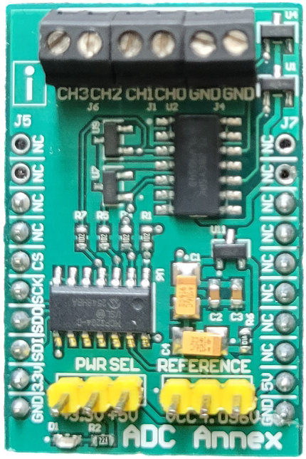
ADC Add-on Board
Request a quoteThe Ikainex™ ADC add-on board is designed for precision analog-to-digital conversion. Powered by Microchip's MCP3204 12-bit SAR ADC, it offers a 4-channel single-ended setup with a fast 100 ksps sampling rate and an SPI-compatible interface. Ideal for industrial monitoring, instrumentation, and remote data acquisition systems.
Key Features
- 12-Bit 4-Channel ADC — Driven by the Microchip MCP3204, supporting up to four single-ended input channels (CH0–CH3).
- Onboard Signal Buffering — Every analog input passes through a TI TLV9054IDR 5MHz rail-to-rail op-amp for optimal signal conditioning before conversion.
- Flexible Reference Selection — Easily switch the reference voltage using the onboard REFERENCE jumper between VCC (3.3V/5V) or an ultra-stable 4.096V provided by the onboard Microchip MCP1541 voltage reference.
- 4-Wire SPI Communication — Supports standard SPI modes (0 and 3) at clock speeds up to 2 MHz, activated via a low CS line.
- Dual Logic Voltage Support — Integrated PWR SEL jumper enables seamless operation with both 3.3V and 5V host microcontrollers.
- Convenient Connectivity — Dedicated CH0–3 terminal blocks with twin GND connections simplify external analog sensor integration.
Overview #
The Ikainex™ ADC is a high-precision analog-to-digital converter expansion board powered by Microchip’s MCP3204 12-bit, 4-channel A/D converter with a fast SPI serial interface. Designed for reliable signal conversion in industrial, instrumentation, and data acquisition applications, it combines flexible reference selection, integrated signal conditioning, and dual-voltage MCU compatibility.
Technical Specifications #
| Parameter | Specification |
|---|---|
| Module Type | 4-Channel, 12-bit ADC |
| ADC | MCP3204, 12-bit A/D converter with SPI interface |
| Analog Inputs | 4 × single-ended channels |
| Resolution | 12-bit |
| Sampling Rate | Up to 100 kSPS |
| Analog Front-End | 4 × operational amplifier channels |
| Op-Amp | TLV9054IDR, 5 MHz rail-to-rail I/O operational amplifier |
| Voltage Reference | MCP1541 precision voltage reference |
| Reference Voltage | 3 selectable reference voltage options |
| Interface | SPI |
| Input Voltage | 3.3 V or 5 V |
| Power Consumption | Low-power operation |
| Board Size | 42.9 × 25.4 mm |
| Primary Applications | Data acquisition, instrumentation, sensor interfacing, embedded systems, and industrial applications |
Pin Configuration #
The following table provides a starting point for documenting the exposed header signals.
                            Pin Header
                       ┌─────────────────┐
                   1   │ NC          NC  │ 20
                   2   │ NC          NC  │ 19
                   3   │ NC          NC  │ 18
                   4   │ NC          NC  │ 17
  SPI chip select  5   │ CS          NC  │ 16
        SPI clock  6   │ SCK         NC  │ 15
     SPI Data Out  7   │ SDO         NC  │ 14
      SPI Data IN  8   │ SDI         NC  │ 13
     Power Supply  9   │ 3.3V        5V  │ 12  Power Supply
           Ground 10   │ GND        GND  │ 11  Ground
                       └─────────────────┘
Board Configuration & Indicators #
| Label | Name | Type | Default | Description |
|---|---|---|---|---|
| LD1 | PWR | LED | — | Power indicator. Turns on when the board is powered. |
| J1 | REFERENCE | Jumper | Left | Selects the ADC reference voltage: VCC (Left) or 4.096 V (Right). |
| J2 | PWR SEL | Jumper | Left | Selects the board’s power/logic level: 3.3 V (Left) or 5 V (Right). |
ADC Electrical Characteristics #
| Parameter | Min | Typ. | Max | Unit |
|---|---|---|---|---|
| Supply Voltage | 3.3 | — | 5.0 | V |
| Analog Supply Voltage | 2.7 | — | 5.5 | V |
| Sampling Rate | 50 | — | 100 | kSPS |
| ADC Resolution | — | — | 12 | bits |
Software Support #
Software examples are available for STM32F446RE and Arduino platforms.
STM32F446RE #
Example firmware demonstrating SPI communication and ADC data acquisition using the STM32F446RE.
Interface: SPI
Language: C
Arduino #
Example sketches demonstrating SPI communication and basic ADC operation with Arduino.
Interface: SPI
Language: C++
Tutorials & Videos #
Tutorial videos are currently being prepared and will be added to this page as they become available.
🎥 Video Tutorials — Coming Soon #
We are preparing step-by-step tutorials covering:
Hardware Setup · SPI Configuration · STM32F446RE · Arduino · ADC Data Acquisition
Videos will be published here soon.
Hardware Resources #
TLV9054IDR Datasheet
Datasheet for the TLV9054 quad rail-to-rail input/output operational amplifier, including electrical characteristics, specifications, pin configuration, applications, and device information.
Download Datasheet (PDF) →MCP1541 Datasheet
Datasheet for the MCP1541 precision voltage reference, including reference-voltage specifications, electrical characteristics, pin configuration, and application information.
Download Datasheet (PDF) →MCP3204 Datasheet
Datasheet for the MCP3204 12-bit, 4-channel analog-to-digital converter with SPI interface, including electrical characteristics, timing specifications, pin configuration, and application information.
Download Datasheet (PDF) →Schematics
Complete electrical schematic, including power, wireless module, connectors, programming/debugging, status indicators, and supporting circuitry.
Download Schematics (PDF) →How to Order #
To order the ADC Add-on Board, send us your required quantity and delivery details. We will confirm availability, lead time, shipping, and the final price before processing your order.
- Submit your contact details and requirements using the quote request form.
- Review the quotation and delivery information we send you.
- Confirm the order with our team.